SOT package refers to the abbreviation of "Small Outline Transistor", which is a form of integrated circuit packaging. SOT package is a surface mount technology (Surface Mount Technology, SMT) package, commonly used in small semiconductor devices, such as transistors, diodes and integrated circuits.
The small size and lightweight profile of the SOT package make it suitable for space-constrained electronic equipment and high-density circuit board designs. It is arranged on both sides of the package through the bending of the pins, which makes soldering easier. SOT packages are usually soldered using surface mount technology, which allows components to be mounted directly on the surface of the board without the need for insertion through apertures.
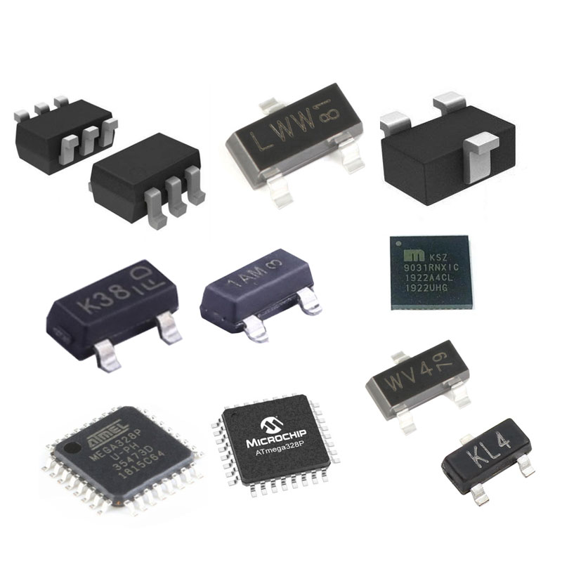
SOT packages come in a variety of sizes and pin configurations, and common types include SOT-23, SOT-89, SOT-223, and more. Each package type has a specific pin count and arrangement to accommodate different device requirements.
Package Features
SOT package (Small Outline Transistor Package) has the following main features:
1. Small size: Compared with the traditional packaging form, the size is smaller and the volume is light. This makes the SOT package ideal for applications in space-constrained electronic devices such as mobile devices, wireless sensors, and portable electronics.
2 surface mount technology: usually surface mount technology (Surface Mount Technology, SMT) for welding. This technique allows components to be mounted directly on the surface of the board without the need for insertion through apertures. Surface mount technology simplifies the production process and improves production efficiency.
3. High pin density: It has a high pin density, especially compared to some traditional plug-in packages. Pins are usually arranged in double or multiple rows, allowing more pins to be connected in a smaller package space, providing more functions and connection options.
4. Thermal performance: Due to the small size, the heat transfer path inside the package is relatively short, which is helpful for heat dissipation. This is sufficient for some low power or small semiconductor devices, but for high power devices or applications in high temperature environments, additional heat dissipation may be required.
5. Lower production cost: Compared with some larger size or high-level packaging forms, the production cost of SOT packaging is usually lower. This is due to factors such as the small package size, the use of less material, and the relatively simple manufacturing process.
Packaging process
The SOT packaging process can be simply summarized as the following steps:
1. Chip preparation: First, the chip to be packaged needs to be prepared. This includes dicing the wafer into individual chips and performing the necessary pre- and post-processing steps, such as metal deposition, etching, diffusion, ion implantation, etc., to form circuit structures and components.
2. Solder ball/pad preparation: For SOT packages, it is usually necessary to install solder balls or pads on the pins of the package. Solder balls/pads are connection points for soldering to the board and can be
The package can be connected to the circuit board by soldering techniques. Solder balls/pads can be prepared by metal evaporation, electroplating, or other processes.
3. Chip positioning and pasting: Position the chip on the package substrate and fix it with an adhesive. The package base is usually made of plastic or ceramic material, which provides the function of supporting and protecting the chip.
4. Welding: In the SOT packaging process, the commonly used welding method is surface mount technology (SMT). The pins are connected to pads or balls on the board by aligning the package with the board and placing it in a predetermined position, followed by soldering using methods such as heat or ultraviolet light.
5. Cleaning and testing: After the packaging is completed, cleaning and testing are carried out to ensure quality and reliability. The cleaning process removes contaminants or residues created during the encapsulation process. Inspection includes visual inspection, pin connectivity testing, performance testing, etc. to ensure that packaged devices meet specifications and standards.
6. Packaging and packaging: Finally, place the packaged chip in a protective box (Tray) or cassette (Tape and Reel) for easy transportation and storage. These are well packaged
The chips can be supplied directly to electronics manufacturers for assembly into larger electronic products.
Eurotech is a worldwide supplier and exporter of electronic components, specializing in ICs, LCDs, Memory, Chips, computer parts, networking equipments and other passive components.
Tel: (86) 755 8395 9469
E-mail: info@eurotech-ic.com