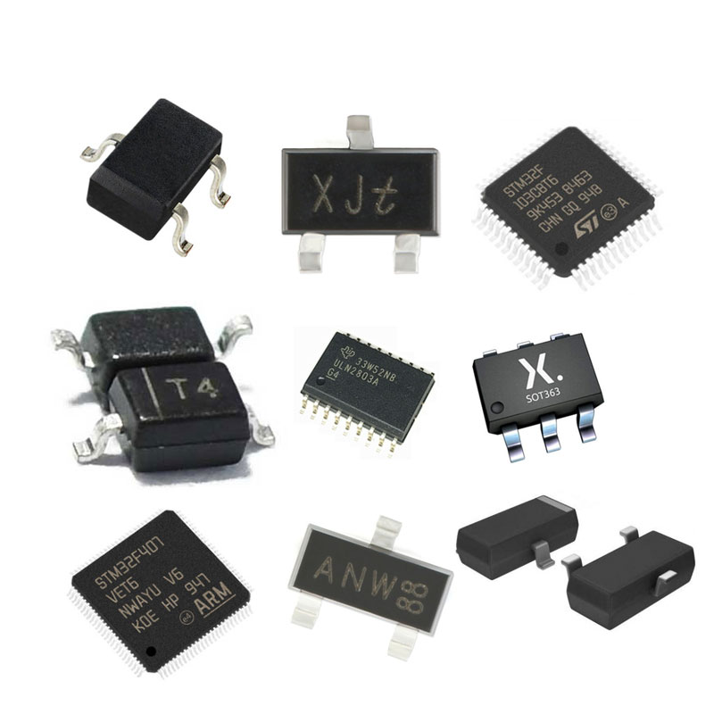
PGA is the abbreviation of "Pin Grid Array", which means "Pin Grid Array". PGA packaging is an electronic component packaging technology, commonly used in the packaging of integrated circuits (IC) and processors. In the PGA package, the pins are located in The bottom of the chip forms a regular grid-like arrangement for connection with the base or socket.
In the PGA package, the pins of the chip are inserted into the holes in the base or socket through short and thin metal pins, so that the chip is connected to the circuit board or other equipment. These pins are usually made of metal or alloy, which can provide a good electrical connection and mechanical support. A major advantage of the PGA package is its good reliability and durability. Since a strong physical connection is formed between the pins and the socket, the chip is not easy to loosen or fall out. This package is also capable of efficiently delivering high-speed signals and power, making it widely used in high-performance applications.
A typical application of PGA packaging is processor packaging. For example, the central processing unit (CPU) used in many desktop computers and servers is often packaged in a PGA, where the pins of the chip plug into a motherboard through a socket. This packaging method can provide good heat dissipation performance and enable the processor to be easily replaced or upgraded.
It should be noted that PGA packaging has different characteristics and applicable scenarios compared with other packaging technologies, such as ball grid array (BGA) and bare chip packaging (CSP). Each package has its own unique advantages and limitations, and it is important to choose the package that suits the needs of a specific application.
process flow
The process flow of PGA packaging includes the following main steps:
1. Design and layout: According to the chip design requirements, carry out the design and layout of the PGA package. This includes determining the number, location and arrangement of pins, and the
with the physical layout of the package.
2. Substrate preparation: Prepare the substrate required for packaging (usually a ceramic or plastic substrate). Substrate preparation includes steps such as dicing, polishing, and metallization.
3. Chip sticking: place the chip on the substrate and fix it in the designated position with an appropriate adhesive. The adhesive is usually thermally conductive to improve heat dissipation. 4. Soldering: To establish an electrical connection between the pins of the chip and the substrate. This can be achieved by soldering techniques, commonly using solder balls or pads. Soldering techniques can be performed manually or using automated equipment.
5. Packaging material: Fill packaging material around the chip and between the pins to provide mechanical support and protect the chip. Common encapsulation materials include epoxy or silicone. 6. Pin shaping: Shaping the pins to ensure that they conform to the standard shape and length. This usually involves cutting, bending or trimming of the leads.
7. Testing and verification: The packaged chip is tested and verified to ensure that it functions properly and meets quality standards and specification requirements. Testing may include electrical performance testing, temperature testing, and reliability testing, among others.
8. Encapsulation of finished products: Finally, the finished products of PGA packaging can be marked, packaged and classified to facilitate storage, transportation and use.
Package Features
The PGA package has the following characteristics:
1. Pin reliability: Use pins or sockets to connect the chip and the circuit board to form a solid physical connection, so it has high pin reliability. The plugging operation between the pin and the socket is not easy to cause damage or loosening of the pin.
2. Heat dissipation performance: The pins are located at the bottom of the chip and can be directly in contact with the heat sink or heat dissipation module to effectively transfer heat. This helps improve the thermal performance of the chip, allowing it to cool better in high-power applications.
3. Easy replacement and maintenance: Due to the connection method between the PGA package chip and the socket, the chip can be replaced or repaired relatively easily. If there is a failure or an upgrade is required, just plug and unplug the chip without complicated soldering operations.
4. Good electrical performance: The pin contact area is larger, which can provide better electrical connection and signal transmission capabilities. This is very important for high-speed signal transmission and power transfer
Therefore, the PGA package is widely used in high-performance applications.
5. Versatility: It can be applied to various integrated circuits and processors, including central processing unit (CPU), graphics processing unit (GPU), digital signal processor
(DSP), etc. This packaging technology is versatile and applicable to different types of chips and application fields.
6. Relatively low cost: Compared with other high-density packaging technologies (such as BGA), the manufacturing cost of PGA packaging is relatively low. It does not require complicated welding and packaging equipment, nor does it require special substrate preparation processes, so it has economic advantages in some application scenarios.
Eurotech is a worldwide supplier and exporter of electronic components, specializing in ICs, LCDs, Memory, Chips, computer parts, networking equipments and other passive components.
Tel: (86) 755 8395 9469
E-mail: info@eurotech-ic.com