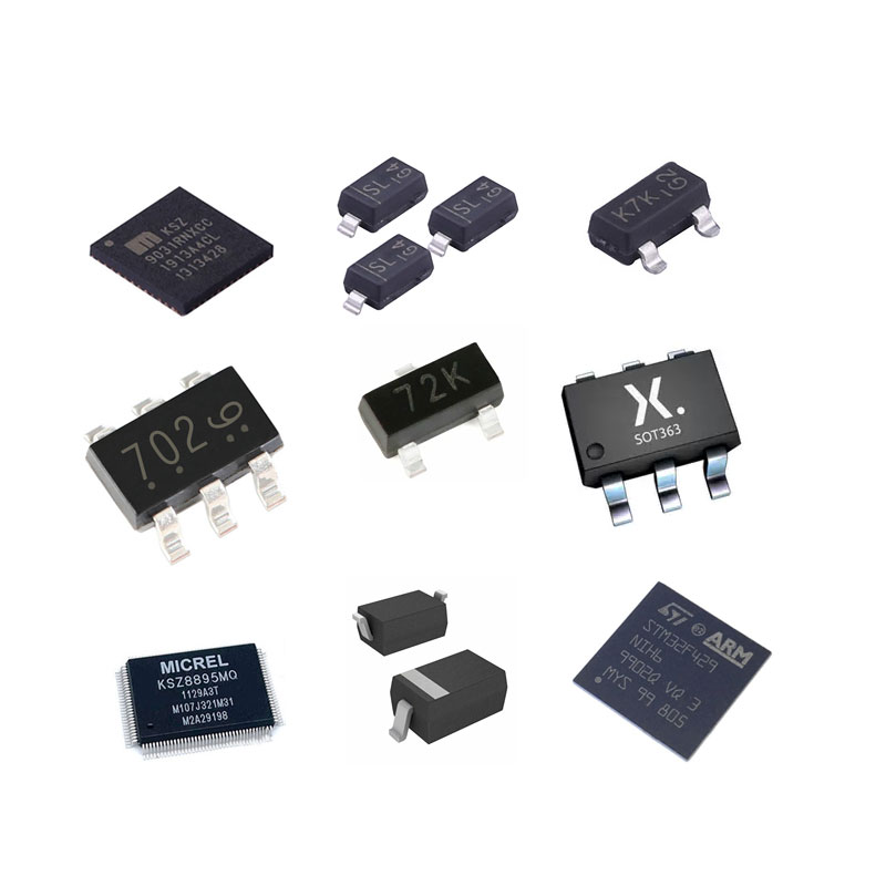
SIP (System in Package) packaging is an integrated circuit (IC) packaging technology that combines multiple chips, devices or modules in one package to form a fully functional system. SIP packaging provides higher integration and performance and reduces system-level connections and size by integrating within the same package.
SIP encapsulation is widely used in various applications, such as mobile devices, wireless communication, Internet of Things, medical equipment, etc. It provides higher performance, smaller size and lower cost, promoting the development and application of integrated circuits.
SIP encapsulation has the following main features:
1. Highly integrated: Allows multiple chips or devices to be integrated in one package to achieve highly integrated functions. These chips or devices may include processors, memories, sensors, wireless modules, radio frequency devices, and the like. Through integration, different functional units can work closely together to achieve more efficient collaborative work.
2. Size optimization: The size of the system can be significantly reduced. By integrating multiple components within a single package, connection lines and space requirements between different components can be eliminated. This helps shrink the entire system into a smaller volume and implement complex functions in a compact space.
3. Signal integrity: Due to the short distance between chips or devices in the SIP package, the signal transmission path is short, which can reduce interference and loss during signal transmission. this
Helps improve signal integrity and reliability.
4. Cost-effectiveness: Although SIP packaging requires multi-chip assembly and testing during the packaging process, compared with the method of separately packaging and connecting multiple chips, SIP packaging can reduce the cost of assembly and connection. In addition, SIP packaging can also reduce the use of system-level connectors, cables and printed circuit boards (PCB), thereby reducing the overall cost of the system.
The process flow of SIP (System in Package) packaging can be summarized as follows:
1. Chip selection and design: Select a chip or device suitable for packaging, and carry out corresponding design and layout. This involves identifying functional and performance requirements, selecting the appropriate chips, and combining them into a single package.
2. Chip processing and packaging: chip processing includes front-end processing and back-end processing. Front-end processing involves etching, deposition, photolithography and other processes on the wafer to form a functional chip. Back-end processing includes cutting, grinding, metallizing, welding and other processes of the chip, and connecting the chip to the packaging substrate or carrier.
3. Packaging design and layout: According to the size of the chip, pin layout and packaging requirements, the packaging design and layout are carried out. This includes determining the shape, size, pin location, number of pins, etc. of the package.
4. Encapsulation material and process: select the appropriate encapsulation material and carry out the encapsulation process. Packaging materials may include substrate materials, solder, packaging glue, heat dissipation materials, and the like. The packaging process includes process steps such as printing, mounting, welding, and curing of packaging glue.
5. Connection and packaging test: During the packaging process, the connection of the pins and the testing of the package are required. Pin connections can be made by soldering or other connection techniques. Package testing includes inspection and verification of the electrical performance, reliability and appearance of the package.
6. Post-package testing and packaging: After packaging, final packaging testing is required, including functional testing, reliability testing, and temperature testing. After the test is completed, the packaged chips are packaged, including steps such as marking, packaging and sealing, and labeling.
7. Finished product inspection and quality control: carry out finished product inspection and quality control on the final SIP packaged products to ensure that the products meet quality requirements and standards. This may include visual inspection, electrical performance testing, reliability testing, etc.
The above is the general process flow of SIP packaging, which may be different for different manufacturers and applications. These steps require strict process control and quality management to ensure package performance, reliability and consistency.
Eurotech is a worldwide supplier and exporter of electronic components, specializing in ICs, LCDs, Memory, Chips, computer parts, networking equipments and other passive components.
Tel: (86) 755 8395 9469
E-mail: info@eurotech-ic.com