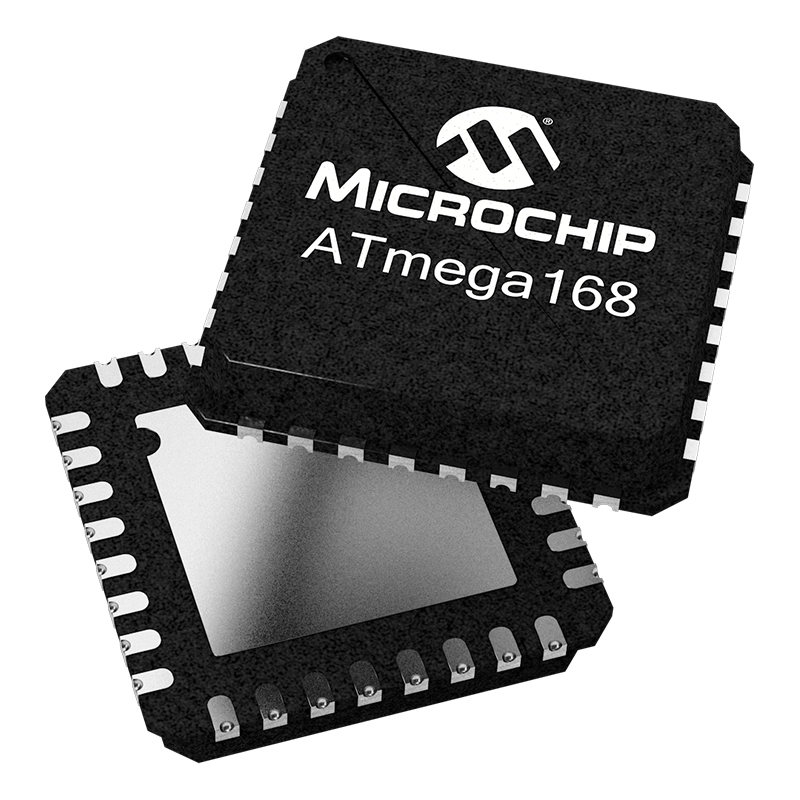
COB (Chips on Board) packaging is a chip packaging technology, also known as wired printed board (COB) packaging. It is to directly install chips (chips without housing) on the printed circuit board, and then use gold wires or copper wires to connect the chip pins to the contact points of the printed circuit board.
In the COB package, the pins of the chip are connected to the copper wires on the printed circuit board through lines, and no additional accessories such as shells or brackets are required. COB packaging technology can package the chip in a very small volume, which improves the reliability and production efficiency of the product, and can also adapt to the application requirements of many different fields.
COB packaging has the advantages of small size, light weight, high reliability, and low cost, and is widely used in microelectronic devices and portable electronic products.
COB packaging process
The process flow of COB packaging generally includes the following steps:
1. Miniature printed circuit board (PCB) design: design the shape, size, wiring and pin position of the printed circuit board
2. Die cutting: cut the chip from the chip wafer to get the die.
3. Die marking: Mark an identification code on each die for future traceability.
4. Bare chip surface treatment: Coat the surface of the bare chip with conductive glue so that the pins of the chip can be connected with the circuit of the printed board.
5. Place the bare chip on the printed circuit board, and use a precision machine to connect the pins of the chip with the circuit board's lines.
6 Metal wire or copper wire connection: Use wires to connect the pins of the chip with the connection points of the printed circuit board, usually using soldering or electronic adhesives for connection 7. Soldering: Use a hot air or infrared welding machine, at the wiring Melt the wires and bond them to the PCB.
8. Circuit board summer cover: Use silica gel or packaging glue to cover the entire chip and its circuits to protect the chip and exposed pins and wires
9. Chip test: Conduct electrical performance test on the packaged chip to ensure that the chip works normally.
10. Sample assembly: Assemble the tested chips into samples or batch operation products.
COB packaging has the following salient features:
1. Small size: COB packaging technology can be used to package the chip in a very small volume to achieve ultra-miniature design, which is suitable for the application requirements of micro electronic devices. 2. Light weight: no additional shell or bracket is required, making The overall chip is lighter and more flexible in design and layout.
3. High reliability: COB packaging technology directly packages the chip on the printed circuit board, there is no contact point between the chip and the pin, which reduces the problems of oxidation, mechanical fatigue and temperature stress, and improves the reliability of the product .
4. Low cost: Since the COB package omits components such as shells and brackets, the production cost is lower, especially in large-scale production.
5. Wide range of application: COB packaging technology is suitable for various chip types, such as ARM, DSP, microcontrollers, etc., and can meet the needs of many different fields. It is one of the most widely used packaging technologies at present.
6. Customizable: It can be customized according to customer needs to adapt to various application scenarios and design requirements.
Eurotech is a worldwide supplier and exporter of electronic components, specializing in ICs, LCDs, Memory, Chips, computer parts, networking equipments and other passive components.
Tel: (86) 755 8395 9469
E-mail: info@eurotech-ic.com