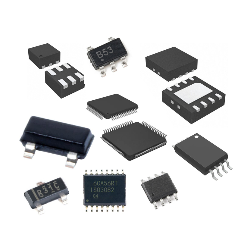
Packaging refers to connecting the circuit pins on the silicon chip to the external joints with wires to connect with other devices. The packaging form refers to the shell used to install the semiconductor integrated circuit chip. It not only plays the role of installing, fixing, sealing, protecting the chip and enhancing the electrothermal performance, but also connects the contacts on the chip to the pins of the package shell with wires, and these pins pass through the wires on the printed circuit board. Connect with other devices to realize the connection between the internal chip and the external circuit. Because the chip must be isolated from the outside world to prevent impurities in the air from corroding the chip circuit and causing electrical performance degradation.
On the other hand, packaged chips are also easier to install and transport. Since the quality of the packaging technology also directly affects the performance of the chip itself and the design and manufacture of the PCB (printed circuit board) connected to it, it is very important.
An important indicator to measure whether a chip packaging technology is advanced is the ratio of chip area to package area, and the closer this ratio is to 1, the better. The main factors to consider when packaging:
1. The ratio of chip area to package area should be as close to 1:1 as possible to improve packaging efficiency;
2. The pins should be as short as possible to reduce the delay, and the distance between the pins should be as far as possible to ensure non-interference and improve performance;
3. Based on heat dissipation requirements, the thinner the package, the better.