
The production of a chip is often divided into four steps: chip design, chip manufacturing, chip packaging and testing. The chip design can be divided into two parts, one is the chip front-end design, and the other is the chip back-end design. The chip front-end design process has to go through repeated comprehensive verification by chip engineers and various design rule checks. In this process, not only must the correctness of the design be ensured, but also the feasibility of the layout and wiring of the design must be ensured, and even further optimized. The back-end design of the chip is the realization of the front-end design. It can be said that the logical synthesis is converted into a physical netlist, and then converted into a graphic file that can be used by the manufacturing plant to manufacture the mask.
Chip manufacturing is mainly divided into purification, ingot manufacturing, slicing, grinding and polishing, oxidation, photolithography and etching. The production line of a chip involves about 2000 to 5000 processes. More comprehensively, wafer production includes two major steps of ingot manufacturing and wafer manufacturing, plus the wafer needle testing process, which can be collectively referred to as wafer Manufacturing front-end process.
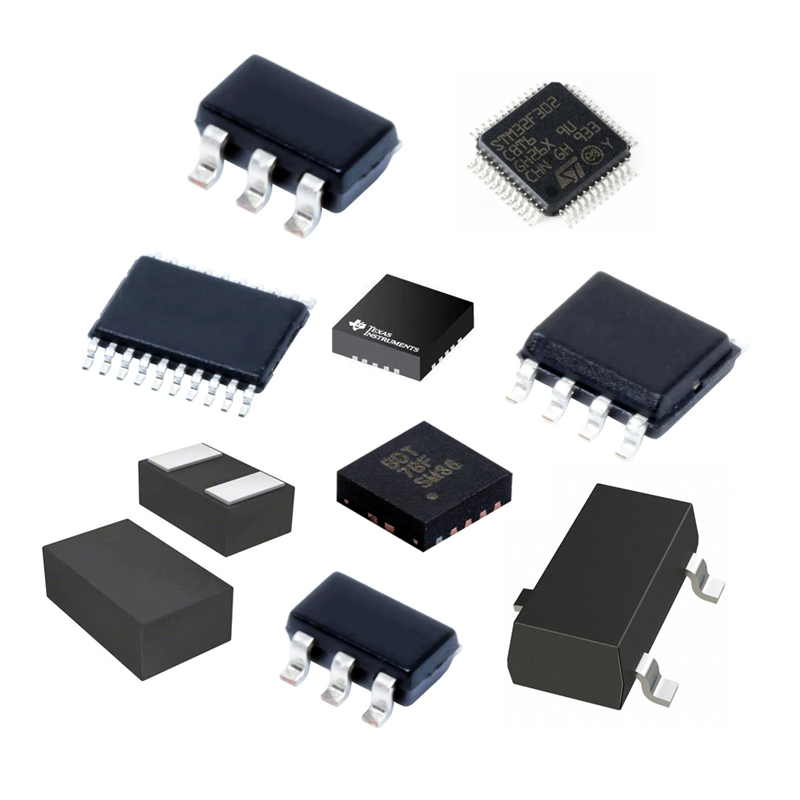
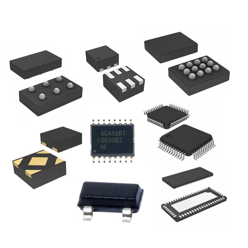
Chip packaging and testing can be collectively referred to as chip packaging and testing. Chip packaging is the process of processing only wafers that pass the test to obtain chips, while testing is to detect those bad chips, including wafer testing and product testing before packaging, so that the yield rate of chips can be improved. As the last step before chip production, chip packaging and testing is crucial to the chip industry. Chip packaging can protect, support, connect, and dissipate heat for the chip, while chip testing can ensure the quality of the chip, and even improve the quality of chip shipments to prevent defective chips from entering the market.


